CCD Sensors in scanners and digital cameras
In almost all flat bed scanners, filmscanners and digital cameras, CCD sensors are applied either in form of CCD lines or CCD chips. One can understand one's scanner or digital camera very much better by looking into the subject that is the core piece. The following chapter provides a detailed insight into the structure and the basic functionality of the CCD elements.
The first three subchapters about semiconductors and the photography effect are very theoretical and only important for those who want to look very deeply into the interior of a CCD element. The chapter about A/D-convertors is very important to me, as it explains the essential connection between the A/D-conversion and the stated colour depth. The following chapters show in a detailed way how a CCD line is structured in a scanner or how a CCD chip is structured in a digital camera.
Semiconductor - Basics and Dopings
Semiconductors are materials which conductance is between very well conducting metals and insulators. In order to influence the conductance of the semiconductors specifically and/or to control it, these are impurified; in the technical terminology, this is called Doping. During the doping, foreign atoms of a deviant quality rating are inserted into a firm crystal structure.
An atom consists on a firm atomic core, in which there is a certain amount of positively charged protons and neutral neutrons and the atomic shell, in which there are the same amount of negatively charged electrodes as the amount of protons located in the core. Due to this, an atom is always neutral. If in the following text I speak about the elements silicon (Si), phosphor (P) and boron (B), then it is about some neutrally charged atoms, thus no positive or negative ions. In the Periodic Table of the Elements, there is silicon in the fourth group, that means that silicon has 4 electrons in its outer atomic shell. Phosphor is in the fifth group, thus it has 5 electrons in the outer atomic shell; and boron is in the third group, thus an element with 5 electrons in the outer shell.
The basis of many semiconductors is silicon. In a crystal of silicon there is a firm structure consisting of single silicon atoms. Each atom has 4 electrons in its outer atomic shell, that are called Valence Electron. On each side of the atom, (visually speaking) a valence electron connects with the respective electron of the neighbouring element and issues with it a firm electronic connection. By this way, each atom forms four firm electronic connections with their neighbouring atoms.
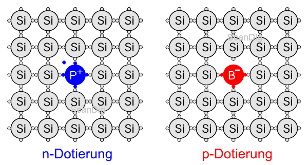
n-Doping
If a silicon crystal is impurified with a pentavalent element as phosphor, the phosphor atom can integrate itself into the silicon-crystal-structure without any problems. But a phorphor atom has 5 valence electrons, from which only 4 can enter a firm convalent bond with the neighboured silicom atoms. Thus, one electron remains that - casually speaking - buzz helpless around because it does not find any partner.
Thus, the phosphor atom that was pressed into the silicon crystal forms a kind of impurity with an excessive electron. The phosphor impurity is called a Donor, thus, it willingly releases an electron. The negatively doped semiconductor is called n-semiconductor. In practice, the structure is as follows: for example, for each million silicon atoms, there is one phosphor atom. Thus, the impurity of the silicon through the phosphor is very slight.
p-Doping
During the p-Doping, a silicon crystal is impurified by a trivalent element as boron. A boron atom has three electrons in its outer electron path, but it actually needs four electrons in order to enter to a covalent bond with each of its neighbouring elements. In turn, casually speaking, now the three electrons of the boron element "argue" to attract the favour of the four partner electron of the silicon atoms. At this point, a hole is remaining there where the electron is missing.
As a result of this electron hole, this impurified crystal is called p-semiconductor. The electron holes would like to gather an electron in order to become neutral. Due to this reason, the boron impurities are also called Acceptors.
Semiconductor - p/n-Junction and Rectifier
What happens now if a p-doped semiconductor is connected to an n-doped semiconductor and/or one half of a silicon crystal is doped with phosphor and the other one with boron, thus producing a p/n-Junction? In the n-doped semiconductor there is an excession of electrons; in the p-doped semiconductor there are (positively charged) electron holes. As each of the atoms always aspire to fill their outer shell with 4 electrons, the excessive electrons on the n-lay migrate into the electron holes of the p-lay. This is why it is talked about an Electron Migration, for a short time, a slight electricity flows.
If now the n-semiconductor releases some electrons to the p-semiconductor, then the electron balance of each atomic bond is equal at both sides, but the total-n-crystals have a lack of electrons and the p-doped crystal has too many in its point balance. Consequently, the n-semiconductor charges itself positively while the p-semiconductor charges itself negatively.
What happens? On the one hand, the excessive electrons of the n-semiconductor are attracted by the positively charged impurities of the p-semiconductor. On the other hand, the overall negatively charged p-semiconductor rejects the electrons, as, as known, negative elements do not get along with negative elements. Therewith, the migration of the electrons is blocked. At the contact point between the p- and the n-lay, a Barrier Layeris formed, and an equilibration is generated.
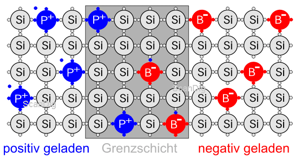
The draft visualizes the formation of a barrier layer. Some excessive electrons migrated from the n-doped layer (left) to the electron holes of the p-doped layer (right) (blue phosphor-electrons an the boron-elements). In the barrier layer, a clean atomic structure is formed, where each atom can enter into four covalent bonds with its neighbouring atoms. At the left side of the barrier layer the phosphor-impurity atoms with excessive electrons are visible and at the right of the barrier layer, there are further boron-atoms with free electron holes. As the left layer is charged positively due to the electrons released to the barrier layer and the right layer is charged negatively due to the electron holes released to the barrier layer, the free electrons of the left layer cannot move any more over the barrier layer. This represents the balanced condition, in which the electron migration comes to a standstill.
Generating a voltage
What happens when a voltage is generated at a p-n-Junction, in which there is already a barrier layer set up? By putting the positively charged n-semiconductor at the positive pole and the negatively charged p-semiconductor at the negative pole of the power source, the excessive electrons of the n-doped semiconductor migrate through the power source into the electron holes of the p-doped semiconductor. Thereby, the barrier layer is amplified and no electricity flows through the silicon-crystal.
To the contrary, by putting the negative pole at the left and the positive pole to the right of the power source, the n-doped layer gets countless electrons from the power source and the electrons are removed from the p-doped layer, so that at the left, there are more excessive electrons and at the right there are more electron holes. Thereby, the barrier layer totally disappears and electricity flows. Thus the p/n-Junction works as a Rectifier (Diode), that lets the electricity flow on one side and block the current flow of the other direction.
Another indication: in the upper draft, the doping of the silicon-crystal with phosphor- and boron-atoms are only presented schematically in the quantity. In order to cope with the practice, I had to draw millions of silicon atoms that are inpurified by one single phosphor- or boron-atom.
The photoelectric effect
In a photodiode, the barrier-layer photo-effect is used to convert light into electric energy. At the light facing side, there is a filmy n-doped layer, thereunder a clearly thicker p-layer. Between these both layers, a barrier-layer is formed as described above. The n-semiconductor-layer is so filmy arranged that the streaming light falls exactly onto the barrier-layer.
The lightbeam might remove an electron of the barrier-layer with its energy. As the p-doped layer is negatively charged due to the formation of the barrier-layer (see above), it rejects the electron and this electron willingly migrates into the positively charged n-layer. The more light incidents on the barrier-layer, the more electrons are rejected by it and collected in the n-doped layer. By connecting the n-layer with the p-layer, electricity flows, this means that the electrons migrate from the n-layer over the electricity circuit to the p-layer. Thus, electricity is generated from the light.
E = h • f
How does a beam manage to remove electrons form a solid electron shell of an atom? According to Max Planck, if light is picked up as a bundle of single Photons, the photon has the energy E = h • f, whereby h is the Planck action quantum. According to the conservation of energy principle, this energy must be sufficient to perform the neccessary electron affinity and to provide the electron with a certain kinetic energy for its further way.
The equation above clarifies that the energy of a photon only depends from the frequency, thus from the colour of the light. The quantity of the electrons released depends on the intensity of the light.
A/D-Converter: From Light over Electricity to a Digital Pixel
In the previous chapter we learned that a photocell converts light in electric energy. Simply expressed, it can be said that at darkness, no electricity flows and at liminosity, a very high electricity flows. In-between there are numerous nuances. In the following drafts, the intensity of current is shown through the brightness of the light, for an easier understanding, I applied a simple grey scale from black to the different shades of grey up to white. Colours will not come into play until the next chapter.
In my drafts I assumed that the intensity of the current increases linearly with the brightness. It does not have to be like this, actually the straight line can be a complicated, quite bulky curve, but this is not important for the following explanation.
Thus, after the light has been converted into electricity, how does the digital image information happen? Now, a A/D-Converter (Analog/Digital-Converter) is applied that converts the analog electricity into a digital signal. At this point it is time to introduce the term Colour Depth that is so commonly used in the Digital Imaging area. An A/D-converter works with a cetain bit-width, that means with a number of bits that indicate the number of the different data.
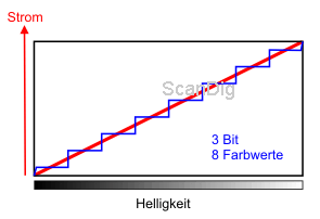
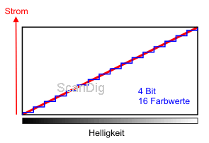
With a 3-Bit A/D-Converter, 23=8 nuances can be generated from the analog current signal, with a 4-Bit-Converter 24=16respectively. Both cases are represented in the drafts above. While a light beam, as also the digital current signal, can have endless nuances of the tonal value, after the A/D-Conversion, only a finite number of nuances remain that can be calculated by the bit-width of the AD-converter.
Therewith, it is clear that the more colour nuances one gets, the more bits has the A/D-converter at the disposal. According to this, a filmscanner with a 36 Bit A/D-converter (12 bits per colour chsnnel) can theoretically differentiate 4096 tonal vlues per colour channel; with a 48 Bit A/D-converter (16 bits per channel), this number increases to 65.536. The bit-width of the A/D-converter if filmscanners is stated as Colour Depth. Thus, it indicates the theoretical maximum number of colour shades that are to be generated with the integrated A/D-Converter. This number has certainly a little relation to the actual colours. This matter is so important to me that I want to emphasize it:
The statement about the colour depth in the case of filmscanners is mostly related to the bid-width of the integrated A/D-converter. It does not indicate the number of the actual producible colours but only a theoretical value that is calculated from the bit-width of the A/D-converter.
Therewith it is also clear that the A/D-converter and/or the whole electronic in a digital camera or a filmscanner plays a decisive role. The A/D-converter does not only have to scan gradually the analog signal but also precisely. The signal processing has an essencial influence to the quality of the image.
Colour Filter Systems
Now, the colour comes into play. We learned in the previous chapter how an A/D-convertor in the black/white area generates digital values of light and / or current signals. Now, a photocell of course does not know any colours, it is practically colour-blind. How can be managed to break the incident light according to the Additive Colour Modell in its three base colours red, green and blue?
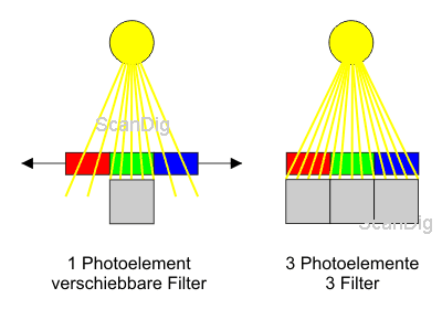
The solution is very simple: by switching the colour filters in front of the photocell, each time one for red, green and blue. But during the technical execution, only one single filter can be put in front of the photo element.
During the so-called three-pass-scanners, the material is scanned three times; thereby, at each pass, another filtering element is put in front of the CCD-elements (see the graphic at the left of the draft). This procedure is indeed possible to realize on a low budget, but therefore it is very slow and also defective, as the advancement motor of a scanner cannot coordinate 100% exactly the three passes; thereby, some unaesthetic colour shifts are generated.
In the so-called single-pass-scanners, for each pixel, three elements are used simultaneously (see the right graphic of the draft above). Each CCD-element has a fix colour filter that cannot be shifted (red, green or blue). Of course, such a sensor is expensive in the production, but the main advantage is the velocity of the scanning.
CCD-Lines of Scanners
In the previous chapter, it was already gone into the difference between three-pass scanners and single-pass scanners. Actually, the three-pass-scanners already belong to the past. All modern scaners and filmscanners work with the single-pass-procedure.
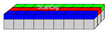
The CCD-line of a scanner consists actually on three lines each having a different colour filter (red, green and blue). According to this, there are three CCD-elements for each pixel, each one with a red, green and blue colour filter at the front. The number of the juxtaposed CCD elements in the sensor cell finally determines the optical resolution of the scanner. But the width of the material to be scanned also plays a decisive role.
Let us assume that in our CCD line, 4000 singles cells are juxtaposed, then the scanner can generate 4000 pixel per line. In a small picture scanner, a line width of 2,5 cm is sufficient, this corresponds approximately to the width of the small picture. As 2,5 cm equal approximately an inch, this ccd line thus generates a scan with approximately 4000 dpi. This equals the optical resolution of the scanner.
The resolution in horizontal direction results from the step size of the transport motor that moves the sensor line a little step forward after each line scan. In case of flat bed scanners, the resolution is willingly given as values of 3000 x 6000 dpi. Hereby, the first number means the optical resolution while the second number represents the step size of the step motor. Only the first number is decisive, as in a scan with 6000 dpi, it must be already interpolated.
The optical resolution of a scanner results form the number of the elements on the CCD-line and the width of the material to be scanned.
The CCD-line must not be as wide as the material to scan. The CCD line described above with 4000 elements can, with its compact format (2,5 cm), also be put into a flat bed scanner that scans materials up to a width of 20 cm. An optical lense system projects then the material of a width of 20 cm to the 2,5 cm of the sensor. Thereby, the resolution falls by the factor 8 to 500 dpi.
The way around, of course, a ccd sensor of a width of 20 cm can be also applied for a small picture film in a flat bed scanner that scans materials of a width of 20 cm (approximately 21,0 cm x 29,7 cm) with 600 dpi, in conjunction with a transparency unit, if the width of 2,5 cm of the small picture are projected to the 20 cm width of the CCD-line. Thereby, the resolution increases to 4800 dpi. It is obvious that with such projections, the quality is affected.
CCD-Chips in Digital Cameras
Where is the essential difference between a filmscanner and a digital camera? The fact that in the case of the filmscanner, the image already exists does not make an important difference for the optic to a free picture motif in the nature. The main difference between both systems consists on that in case of a filmscanner, the picture is scanned unhurriedly, line by line, while the digital camera with its short exposure time makes a short snapshot from the whole picture at once.
In order to digitalize a small picture sized 24 x 36 mm, in the case of a filscanner, a sensor line of 2,5 cm with 4000 elements and a respectively accurate step motor is enough, as described in the previous chapter. Therewith, form a small picture model, approximately 4000 x 6000 pixel result, thus more than 20 megapixel. The proceeding of the scanning line by line takes, depending on the scanner, between half a minute to several minutes.
In order to create a complete image in a digital camera in 1/60 s exposure time, no CCD-line with step motor can be applied but only a CCD-chip, on which there are own sensor elements for all pixels. Thus, a CCD-chip consists on a matrix of sensor elements, which number results in the resolution of the camera. Some might already have the picture of a CCD-chip in mind, by copying several times consecutively the CCD line represented in the previos chapter. But far from it, as now, the peculiarities of the digital cameras come into play.
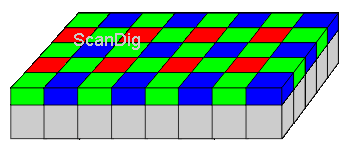
On a CCD chip of a digital camera there are no red, green and blue CCD-elements to each third of a line alternatively. The red, green and blue filter elements are rather checkered, whereby the amount of the green elementsis is of 50%, while the red and blue elements are only represented each by 25%. The reason for such an unbalanced distribution is due to the capacity of the colour perception of the human eye. But now, we come to a big paradox of the digital cameras concerning their resolution. As an example, we take a digital camera with 4 million pixels.
In the previous chapters we learned that for the generation of 4 million pixels, a total of 12 million sensor elements, thus 4 millions of each red, green and blue colour filters are needed. But on a CCD chip of a digital camera there are only 4 million sensor elements in total, therefrom 1 million red, 1 million blue and 2 million green ones. For the processor in the gigital camera, this division into shares and the distribution of the different colours is not a problem, as from this, it generates a clear picture. But this distribution of colours means for the user that in reality, he does not shoot a real 4 pixel picture but in principle only captures 1,33 million of 3-colour-value that is generated to 4 million pixels by the interpolation. It is very important to me to emphasize this:
In a digital camera, the number of the megapixels means the number of the CCD elements with each one having colour filter in front of it. Therefore, the real resolution compared to filmscanners is lower by the factor 3.
Foveon-Sensor
In the case of foveon-sensors, the three colour layers are lying upon each other; each is sensibilized for a certain wavelength range of the light. Thereby, in a faveon-chip, a picture is created without any calculational interpolation, as three colour values are measured for each pixel. Thus, a faveon-chip with 3 megapixels generates 3 million pixels, this is why the producers of digital cameras with faveon-chip like to indicate the total resolution in analogy to the unreal resolutions of the competitor as 3 x 3 megapixels.
Back to the index Know How
|